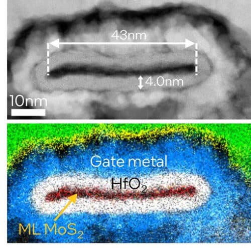
Intel has improved transistor technology by using super thin 2D materials, creating more efficient and smaller devices with new building methods.

Intel researchers have made significant advancements in transistor performance by employing ultra-thin 2D transition metal dichalcogenides (TMDs), such as MoS₂ and WSe₂, for transistor channels. These materials are particularly suited for scaled-down devices due to their outstanding electrical properties. However, integrating these materials into existing technology faces challenges, primarily because these 2D materials lack atomic “dangling bonds”, which are critical for forming strong connections with other materials.
Intel developed specialised techniques to overcome these integration challenges, including a gate oxide atomic layer deposition (ALD) process and a low-temperature gate cleaning method. These innovations have enabled the construction of gate-all-around (GAA) NMOS and PMOS transistors that exhibit unprecedented performance metrics. Notably, these transistors have achieved record values in subthreshold slopes and drain currents, essential metrics for evaluating transistor efficiency and speed.
Notable achievements include MoS₂ NMOS transistors with a subthreshold slope of less than 75 mV/dec and a maximum drain current of over 900 µA/µm. In comparison, WSe₂ PMOS devices achieved a subthreshold slope of 156 mV/dec and a maximum drain current of 132 µA/µm. These results highlight the high-performance potential of monolayer TMDs when integrated into transistor designs.
These technological advancements underscore the promise of 2D TMDs in future electronics, pushing the boundaries of what’s possible in device miniaturisation and efficiency. However, despite the progress, there is a significant need for further research to fully harness these materials’ capabilities and successfully integrate them into mainstream technology. Intel’s achievements mark a pivotal step forward and highlight the ongoing challenges in optimising and deploying 2D materials in electronics.


